Machine Learning-Assisted Design of FinFET-Based Operational Amplifiers and LC Oscillators at the 22 nm Node: A Review
Keywords:
FinFET, High-k dielectric, Operational amplifier, LC oscillator, Machine learning, Linear regression, Analog design automationAbstract
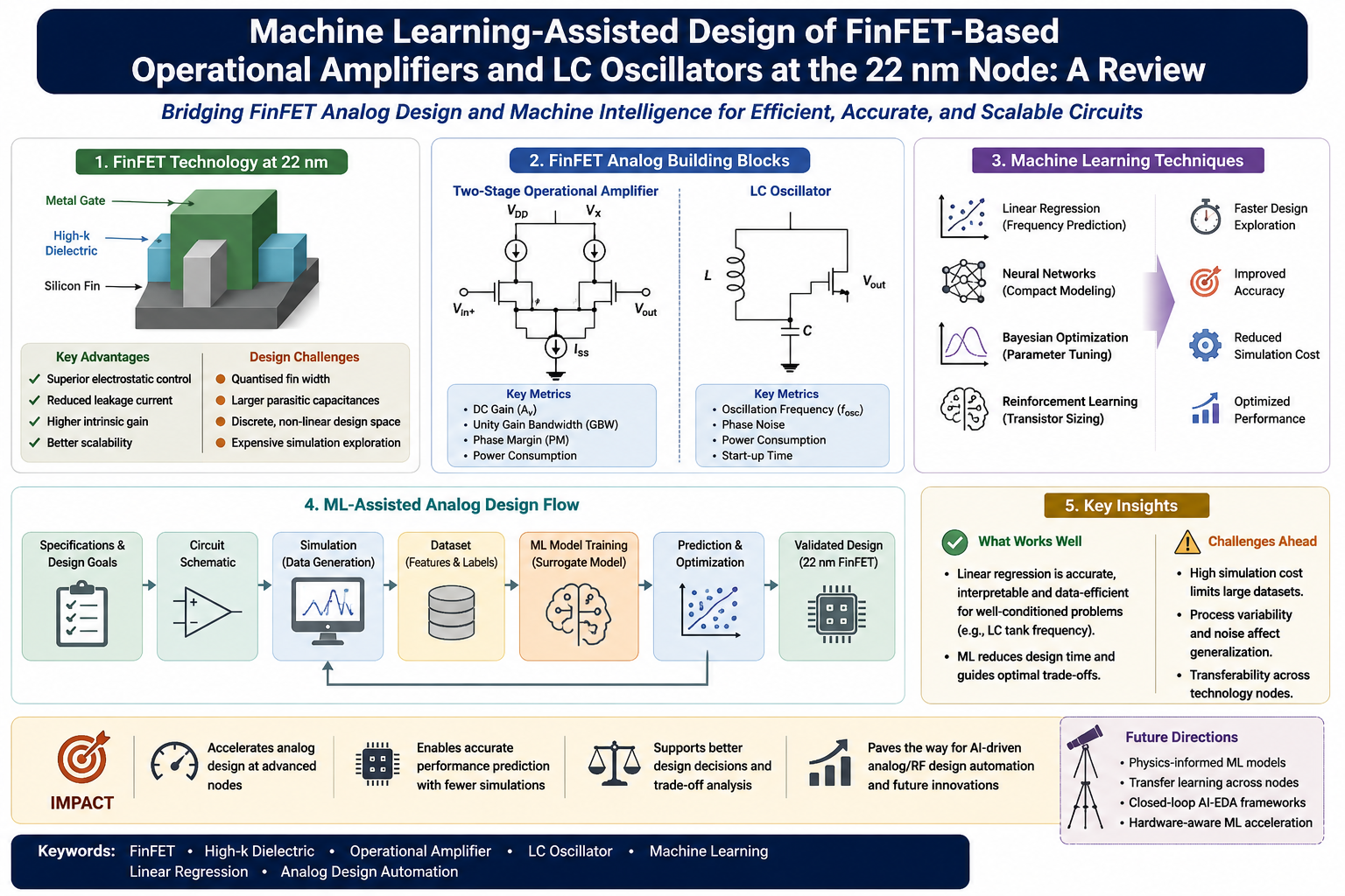
The transition from planar CMOS to fin field-effect transistor (FinFET) technology has reshaped analog and radio-frequency circuit design, offering superior electrostatic control, reduced leakage, and higher intrinsic gain at the 22 nm node, but at the cost of quantised device widths, larger parasitic capacitances, and a design space that is expensive to explore through simulation alone. This paper reviews the convergence of two research directions: FinFET-based analog building blocks, particularly two-stage operational amplifiers realised with high-k gate dielectrics and inductor-capacitor (LC) oscillators, and the growing use of machine learning to model and optimise these circuits. The review first summarises FinFET device physics, high-k/metal-gate integration, and the analog figures of merit that distinguish FinFETs from planar devices. It then examines reported 22 nm FinFET operational amplifiers and LC oscillator designs, and surveys machine learning techniques ranging from linear regression frequency predictors to neural-network compact models, Bayesian optimisation, and reinforcement-learning-based transistor sizing. Comparative tables summarise the method, technology, and key contribution of representative works, and a design flow that couples simulation-derived datasets with learned surrogate models is presented. The synthesis shows that simple regression models already give accurate and interpretable predictions for well-conditioned problems such as LC tank frequency, whereas data-hungry neural and reinforcement-learning approaches remain limited by simulation cost, process variability, and transferability across technology nodes. Open challenges and future research directions are outlined.
References
[1] D. Hisamoto, W.-C. Lee, J. Kedzierski, H. Takeuchi, K. Asano, C. Kuo, E. Anderson, T.-J. King, J. Bokor, and C. Hu, “FinFET-a self-aligned double-gate MOSFET scalable to 20 nm,” IEEE Transactions on Electron Devices, vol. 47, no. 12, pp. 2320-2325, 2000, doi: 10.1109/16.887014.
[2] G. D. Wilk, R. M. Wallace, and J. M. Anthony, “High-κ gate dielectrics: current status and materials properties considerations,” Journal of Applied Physics, vol. 89, no. 10, pp. 5243-5275, 2001, doi: 10.1063/1.1361065.
[3] V. Subramanian et al., “Planar bulk MOSFETs versus FinFETs: an analog/RF perspective,” IEEE Transactions on Electron Devices, vol. 53, no. 12, pp. 3071-3079, 2006, doi: 10.1109/TED.2006.885649.
[4] D. Bhattacharya and N. K. Jha, “FinFETs: from devices to architectures,” Advances in Electronics, vol. 2014, Art. no. 365689, pp. 1-21, 2014, doi: 10.1155/2014/365689.
[5] G. G. E. Gielen and R. A. Rutenbar, “Computer-aided design of analog and mixed-signal integrated circuits,” Proceedings of the IEEE, vol. 88, no. 12, pp. 1825-1854, 2000, doi: 10.1109/5.899053.
[6] S. Decoutere, P. Wambacq, V. Subramanian, J. Borremans, and A. Mercha, “Technologies for (sub-) 45nm analog/RF CMOS - circuit design opportunities and challenges,” in Proceedings of the IEEE Custom Integrated Circuits Conference (CICC), 2006, pp. 679-686, doi: 10.1109/CICC.2006.320879.
[7] L. T. Clark, V. Vashishtha, L. Shifren, A. Gujja, S. Sinha, B. Cline, C. Ramamurthy, and G. Yeric, “ASAP7: a 7-nm finFET predictive process design kit,” Microelectronics Journal, vol. 53, pp. 105-115, 2016, doi: 10.1016/j.mejo.2016.04.006.
[8] A. Dasgupta et al., “BSIM-CMG compact model for IC CAD: from FinFET to gate-all-around FET technology,” Journal of Microelectronic Manufacturing, vol. 3, no. 4, pp. 1-8, 2020, doi: 10.33079/jomm.20030402.
[9] G. Vasudeva, P. Y. Mallikarjun, M. Jatkar, T. R. Kulkarni, R. R. Kulkarni, B. Gururaj, and M. P. Tejas, “Design of OPAMP based on 22 nm FinFET technology,” in Proceedings of the Fifth International Conference on Trends in Computational and Cognitive Engineering (TCCE 2023), Lecture Notes in Networks and Systems, vol. 1208, Singapore: Springer, 2025, pp. 371-382, doi: 10.1007/978-981-96-0185-1_32.
[10] G. Vasudeva, M. Jatkar, T. R. Kulkarni, R. R. Kulkarni, B. Gururaj, and M. P. Tejas, “Design of FinFET based op-amp using high-k device 22 nm technology,” in Applied Mathematics, Modeling and Computer Simulation: Proceedings of the 3rd International Conference (AMMCS 2023), Advances in Transdisciplinary Engineering, SAGE Publications, 2024, pp. 928-939, doi: 10.3233/ATDE231033.
[11] Q.-J. Zhang, K. C. Gupta, and V. K. Devabhaktuni, “Artificial neural networks for RF and microwave design-from theory to practice,” IEEE Transactions on Microwave Theory and Techniques, vol. 51, no. 4, pp. 1339-1350, 2003, doi: 10.1109/TMTT.2003.809179.
[12] R. Mina, C. Jabbour, and G. E. Sakr, “A review of machine learning techniques in analog integrated circuit design automation,” Electronics, vol. 11, no. 3, Art. no. 435, 2022, doi: 10.3390/electronics11030435.
[13] E. Afacan, N. Lourenço, R. Martins, and G. Dündar, “Review: machine learning techniques in analog/RF integrated circuit design, synthesis, layout, and test,” Integration, vol. 77, pp. 113-130, 2021, doi: 10.1016/j.vlsi.2020.11.006.
[14] M. Fayazi, Z. Colter, E. Afshari, and R. Dreslinski, “Applications of artificial intelligence on the modeling and optimization for analog and mixed-signal circuits: a review,” IEEE Transactions on Circuits and Systems I: Regular Papers, vol. 68, no. 6, pp. 2418-2431, 2021, doi: 10.1109/TCSI.2021.3065332.
[15] W. Lyu, F. Yang, C. Yan, D. Zhou, and X. Zeng, “Multi-objective Bayesian optimization for analog/RF circuit synthesis,” in Proceedings of the 55th Annual Design Automation Conference (DAC), 2018, pp. 1-6, doi: 10.1145/3195970.3196078.
[16] H. Wang, K. Wang, J. Yang, L. Shen, N. Sun, H.-S. Lee, and S. Han, “GCN-RL circuit designer: transferable transistor sizing with graph neural networks and reinforcement learning,” in Proceedings of the 2020 57th ACM/IEEE Design Automation Conference (DAC), 2020, pp. 1-6, doi: 10.1109/DAC18072.2020.9218757.
[17] K. Settaluri, A. Haj-Ali, Q. Huang, K. Hakhamaneshi, and B. Nikolic, “AutoCkt: deep reinforcement learning of analog circuit designs,” in Proceedings of the 2020 Design, Automation and Test in Europe Conference and Exhibition (DATE), 2020, pp. 490-495, doi: 10.23919/DATE48585.2020.9116200.
[18] M. Jatkar, G. Vasudeva, T. R. Kulkarni, R. R. Kulkarni, and A. Pandurangi, “LC oscillator frequency prediction using machine learning linear regression algorithm,” Discover Electronics, vol. 2, no. 1, Art. no. 52, 2025, doi: 10.1007/s44291-025-00092-9.
[19] W.-F. Lü and L. Dai, “Impact of work-function variation on analog figures-of-merits for high-k/metal-gate junctionless FinFET and gate-all-around nanowire MOSFET,” Microelectronics Journal, vol. 84, pp. 54-58, 2019, doi: 10.1016/j.mejo.2018.12.004.
[20] F. Silveira, D. Flandre, and P. G. A. Jespers, “A gm/ID based methodology for the design of CMOS analog circuits and its application to the synthesis of a silicon-on-insulator micropower OTA,” IEEE Journal of Solid-State Circuits, vol. 31, no. 9, pp. 1314-1319, 1996, doi: 10.1109/4.535416.
[21] N. Z. Butt and J. B. Johnson, “Modeling and analysis of transistor mismatch due to variability in short-channel effect induced by random dopant fluctuation,” IEEE Electron Device Letters, vol. 33, no. 8, pp. 1099-1101, 2012, doi: 10.1109/LED.2012.2199075.
[22] B. Hesham, E. Hasaneen, and H. F. A. Hamed, “Design procedure for two-stage CMOS opamp using gm/ID design methodology in 16 nm FinFET technology,” in Proceedings of the 2019 31st International Conference on Microelectronics (ICM), 2019, pp. 325-329, doi: 10.1109/ICM48031.2019.9021511.
[23] S. Ferwani, S. Khandelwal, and R. Shrivastava, “Low power FinFET based operational amplifier with improved gain at 45 nm technology regime,” Journal of Nanoelectronics and Optoelectronics, vol. 11, no. 3, pp. 377-381, 2016, doi: 10.1166/jno.2016.1903.
[24] G. Vasudeva and B. V. Uma, “22nm FinFET based high gain wide band differential amplifier,” International Journal of Circuits, Systems and Signal Processing, vol. 15, pp. 55-62, 2021, doi: 10.46300/9106.2021.15.7.
[25] G. Vasudeva and B. V. Uma, “Low voltage low power and high speed OPAMP design using high-K FinFET device,” WSEAS Transactions on Circuits and Systems, vol. 20, pp. 80-87, 2021, doi: 10.37394/23201.2021.20.11.
[26] V. Gowdagere and U. B. Venkataramanaiah, “Operational transconductance amplifier-based comparator for high frequency applications using 22 nm FinFET technology,” International Journal of Electrical and Computer Engineering (IJECE), vol. 12, no. 2, pp. 2158-2168, 2022, doi: 10.11591/ijece.v12i2.pp2158-2168.
[27] S. Dolui, G. Kundu, and J. Basu, “Machine learning based regression model for automated analog circuit design over different transistor regions,” in Proceedings of the 2024 IEEE 21st India Council International Conference (INDICON), 2024, pp. 1-6, doi: 10.1109/INDICON63790.2024.10958405.
[28] D. B. Leeson, “A simple model of feedback oscillator noise spectrum,” Proceedings of the IEEE, vol. 54, no. 2, pp. 329-330, 1966, doi: 10.1109/PROC.1966.4682.
[29] B. Razavi, “A study of phase noise in CMOS oscillators,” IEEE Journal of Solid-State Circuits, vol. 31, no. 3, pp. 331-343, 1996, doi: 10.1109/4.494195.
[30] A. Hajimiri and T. H. Lee, “A general theory of phase noise in electrical oscillators,” IEEE Journal of Solid-State Circuits, vol. 33, no. 2, pp. 179-194, 1998, doi: 10.1109/4.658619.
[31] P. Andreani, X. Wang, L. Vandi, and A. Fard, “A study of phase noise in Colpitts and LC-tank CMOS oscillators,” IEEE Journal of Solid-State Circuits, vol. 40, no. 5, pp. 1107-1118, 2005, doi: 10.1109/JSSC.2005.845991.
[32] C. Zhao, M. Fang, and T. Yoshimasu, “A 14-GHz-band low-supply-voltage low-phase-noise LC-VCO IC with harmonic tuned LC tank in 45-nm CMOS SOI,” in Proceedings of the 2024 21st International SoC Design Conference (ISOCC), 2024, pp. 79-80, doi: 10.1109/ISOCC62682.2024.10762669.
[33] S. Temich, L. Chruszczyk, and D. Grzechca, “Identification of the specification parameters for a voltage controlled oscillator using an artificial neural network with a genetic algorithm,” Elektronika ir Elektrotechnika, vol. 24, no. 6, pp. 42-49, 2018, doi: 10.5755/j01.eie.24.6.20945.
[34] Z. Sun, J. Wei, Q. Wu, and H. Wang, “Machine learning-assisted synthesis of low-phase noise oscillator,” in Proceedings of the 2023 IEEE International Workshop on Electromagnetics: Applications and Student Innovation Competition (iWEM), 2023, pp. 346-348, doi: 10.1109/iWEM58222.2023.10234924.
[35] G. James, D. Witten, T. Hastie, and R. Tibshirani, An Introduction to Statistical Learning with Applications in R, 2nd ed. New York, NY, USA: Springer, 2021, doi: 10.1007/978-1-0716-1418-1.
[36] J. Wang, Y.-H. Kim, J. Ryu, C. Jeong, W. Choi, and D. Kim, “Artificial neural network-based compact modeling methodology for advanced transistors,” IEEE Transactions on Electron Devices, vol. 68, no. 3, pp. 1318-1325, 2021, doi: 10.1109/TED.2020.3048918.
[37] A. Maity, S. K. Maity, and H. S. Das, “A data-driven compact drain current model for InGaAs FinFET using TCAD assisted machine learning approach,” Engineering Research Express, vol. 6, no. 4, Art. no. 045353, 2024, doi: 10.1088/2631-8695/ad980c.
[38] Z. Wu and I. Savidis, “Circuit-GNN: a graph neural network for transistor-level modeling of analog circuit hierarchies,” in Proceedings of the 2023 IEEE International Symposium on Circuits and Systems (ISCAS), 2023, pp. 1-5, doi: 10.1109/ISCAS46773.2023.10181617.
[39] K. Touloupas and P. P. Sotiriadis, “Mixed-variable Bayesian optimization for analog circuit sizing through device representation learning,” Electronics, vol. 11, no. 19, Art. no. 3127, 2022, doi: 10.3390/electronics11193127.
[40] A. F. Budak, P. Bhansali, B. Liu, N. Sun, D. Z. Pan, and C. V. Kashyap, “DNN-Opt: an RL inspired optimization for analog circuit sizing using deep neural networks,” in Proceedings of the 2021 58th ACM/IEEE Design Automation Conference (DAC), 2021, pp. 1219-1224, doi: 10.1109/DAC18074.2021.9586139.
Downloads
Published
How to Cite
Issue
Section
License
Copyright (c) 2026 International Journal of Smart Technologies and Innovations

This work is licensed under a Creative Commons Attribution-NonCommercial-ShareAlike 4.0 International License.
License Terms
The International Journal of Smart Technologies and Innovations (IJSTI) publishes articles under an open-access publishing model to promote the free and global dissemination of scholarly research.
Licensing Policy
Authors publishing in IJSTI agree that:
-
The submitted work is original and does not infringe upon the copyright or intellectual property rights of others.
-
Authors retain copyright of their published articles while granting the journal the non-exclusive right to publish, archive, reproduce, and distribute the work in electronic and print formats.
-
Published articles may be accessed, downloaded, copied, shared, cited, and used for academic, educational, and non-commercial research purposes, provided proper acknowledgment and citation of the original publication are given.
-
Any commercial use, reproduction, or distribution of published content without prior written permission from the journal and/or author is prohibited.
-
Authors are responsible for obtaining permission for any copyrighted materials used in their manuscripts, including images, figures, tables, or third-party content.
-
The journal reserves the right to preserve, archive, index, and distribute published content through scholarly databases, repositories, and digital preservation systems.
-
By submitting a manuscript, authors confirm that all co-authors have approved the submission and agree to the journal’s licensing and publication policies.
Open Access Statement
IJSTI provides immediate open access to its content based on the principle that making research freely available to the public supports greater global knowledge exchange and academic advancement.
Journal Website:
IJSTI Official Website


